Impact of friction-induced microdefects on the surface properties of MoS2

  • Haowen XU 1 ,
  • Zejun SUN 1 ,
  • Rui HAN 1 ,
  • Shihong CHEN 1 ,
  • Chong WANG 1 ,
  • Shuchun HUANG 1 ,
  • Weiqing LI 2 ,
  • Huan LIU 1 ,
  • Dameng LIU , 1, *
Expand
  • 1. State Key Laboratory of Tribology in Advanced Equipment, Tsinghua University, Beijing 100084, China
  • 2. China University of Geosciences, Beijing 100083, China

Received date: 2024-10-28

  Online published: 2025-02-18

Copyright

All rights reserved. Unauthorized reproduction is prohibited.

Abstract

Objective: The rapid evolution of the high-end equipment manufacturing industry, from traditional manual Methods to advanced digital intelligent manufacturing, has significantly improved production precision and contributed to technological advancements across various sectors. As the demand for the reliability and durability of critical components in aerospace, semiconductor manufacturing, and other industries continues to rise, there is an increasing focus on understanding microscale defects caused by friction. These friction-induced microdefects, including microcracks and phase transitions, present significant challenges. Although these defects are often subtle and not easily observed under standard conditions, their cumulative effects can significantly impact material performance. Currently, systematic investigations into the influence of friction-induced defects on the optical properties of semiconducting materials remain limited. Methods: This research addresses this gap by focusing on monolayer molybdenum disulfide (MoS2), a widely studied two-dimensional (2D) material known for its exceptional electronic and optical properties. Monolayer MoS2 samples, free of defects, were prepared through the mechanical exfoliation method. Microscale friction-induced defects were introduced via atomic force microscopy under controlled loading conditions to ensure reproducibility and minimize significant structural damage. After defect introduction, the optical properties were analyzed via photoluminescence (PL) spectroscopy and Raman microscopy. Results: The experimental results showed that friction-induced defects generated new defect energy levels within the MoS2 structure. These defect states served as non-radiative recombination centers, leading to a substantial reduction in PL intensity and exciton lifetime. Steady-state PL measurements showed a significant decrease in fluorescence intensity in defect-affected regions compared with pristine regions. Time-resolved PL spectroscopy further quantified the reduction in exciton lifetime, from 0.198 ns in pristine regions to 0.128 ns in defected regions, confirming that defects introduced non-radiative dissipation channels for excitons. Raman spectroscopic analysis confirmed the structural integrity of the samples after friction, with observable shifts in vibrational modes indicating the presence of localized stress fields and defect-induced modifications. Temperature-dependent PL studies highlighted the pronounced impact of friction defects at low temperatures. As the temperature decreased, defect-induced PL peaks became dominant in the spectral profile, particularly below 60 K; this behavior is attributed to the enhanced capture of excitons by defect states owing to reduced thermal activation at lower temperatures. Moreover, the defect-induced spectral features became more prominent with higher excitation powers, highlighting the influence of the features on carrier dynamics and non-radiative recombination pathways. These results emphasize the critical role of defect management in optimizing the performance of MoS2-based optoelectronic devices. Conclusions: The presence of friction-induced defects not only reduces PL efficiency but also shortens exciton lifetimes, posing challenges for applications that require high quantum yield and stable emission properties. Therefore, strategies to mitigate defect formation during manufacturing and operational processes are crucial for improving device reliability and efficiency. This study elucidates the physical mechanisms driving defect-induced alterations in the optical properties of 2D materials, offering a foundation for improved material design and device engineering. Future research will focus on extending these findings to other 2D materials, such as WS2 and BN, and incorporating advanced characterization techniques, such as electron microscopy and first-principles calculations, to investigate defect formation at the atomic scale. By addressing these challenges, this research plays a key role in advancing the development of next-generation, high-performance optoelectronic devices suited for demanding industrial applications.

Cite this article

Haowen XU , Zejun SUN , Rui HAN , Shihong CHEN , Chong WANG , Shuchun HUANG , Weiqing LI , Huan LIU , Dameng LIU . Impact of friction-induced microdefects on the surface properties of MoS2[J]. Journal of Tsinghua University(Science and Technology), 2025 , 65(2) : 385 -391 . DOI: 10.16511/j.cnki.qhdxxb.2025.21.008

高端装备制造业经历了传统手工制造、自动机床制造和数字智能制造等多个发展阶段,制造精度不断提升,产品一致化与性能迎来了飞跃,同时推动了人类文明向前迈进。随着航空航天、半导体制造、轨道运输和生物医疗等领域对高端装备核心零部件可靠性和耐用性的要求日益提升,界面摩擦引起的微观缺陷逐渐成为研究重点[1-2]。摩擦微观缺陷是摩擦缺陷在微观尺度上的表现,主要是指在材料的微观结构中出现的细微变化。这包括材料表面和次表面的微裂纹、微孔以及由于摩擦引起的相变等现象。这些微小的缺陷可能在正常条件下不易被察觉,但它们的累积效应会对材料的整体性能产生显著影响。
科研人员对微观摩擦磨损特性进行了广泛的研究,比如微观尺度上摩擦缺陷对摩擦力的影响[3],薄膜材料特性对微观摩擦磨损的影响等[4-6]。但是,关于微观缺陷如何影响半导体材料的发光特性的研究仍未被报道,若能深入研究摩擦微观缺陷对材料发光特性的影响,将有助于更加深入理解材料的本质及发光机理,为优化材料性能提供理论基础;同时通过对缺陷的控制,能够设计出更高效、可靠的光电子器件如发光二极管和激光器,满足更高的应用需求[7]
本文通过机械剥离法制备干净、无缺陷的单层二硫化钼(molybdenum disulfide, MoS2)材料,并通过光学显微镜、原子力显微镜(型号NTEGRA, 厂家NT-MDT)、拉曼显微镜(型号LabRAM HR Evolution, 厂家Horiba)等手段对其发光特性进行了表征;使用原子力探针在二维材料表面进行摩擦,以产生微观摩擦缺陷,并再次对含有微观摩擦缺陷的MoS2单层的发光特性进行表征;最后测试了其在不同温度下的光致发光特性,并对微观缺陷影响MoS2发光特性的机理进行了总结。

1 实验方法

1.1 MoS2单层的制备与摩擦微观缺陷制备

为了获得低缺陷浓度且表面干净的二维材料,采用机械剥离法制备了MoS2单层薄片。单层MoS2的光学图片如图 1a所示,为了后续通过原子力探针摩擦产生微观缺陷,样品并未用氮化硼(hexagonal boron nitride, hBN)进行封装。图 1b展示了单层MoS2引入摩擦微观缺陷与未引入摩擦微观缺陷的区域的原子力显微镜图像。
图 1 单层MoS2的表征与摩擦微观缺陷对Raman峰的影响
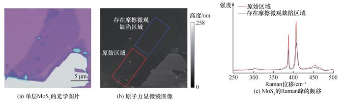
通过原子力显微镜在单层MoS2表面引入微观缺陷,选用弹性系数为32 N/m的AC160Ts探针。为确保实验可重复性并避免样品破损,施加载荷设为1 500 nN,此参数基于前期实验优化得出。在原子力显微镜的接触模式下,在选定的样品区域进行往复扫描摩擦。本文在选择探针和施加载荷时所选定的标准已被验证能引入微观缺陷且不会对单层MoS2造成破损;通过前期实验确定施加载荷处于摩擦引起微观缺陷的阈值范围内,同时避免产生明显的塑性变形或裂纹;摩擦实验结束后,通过Raman光谱对样品进行了表面结构完整性验证,未发现明显的Raman特征峰消失现象,表明样品未发生破损。
Raman显微镜被用于对摩擦前后的单层进行表征,以验证微观摩擦缺陷的形成。使用Raman显微镜进行表征,并通过532 nm波长激光,通过一个100倍物镜(数值孔径0.9 NA, 厂家Olympus)聚焦至样品,激光功率为440 μW。

1.2 对引入微观缺陷的MoS2单层发光特性的表征

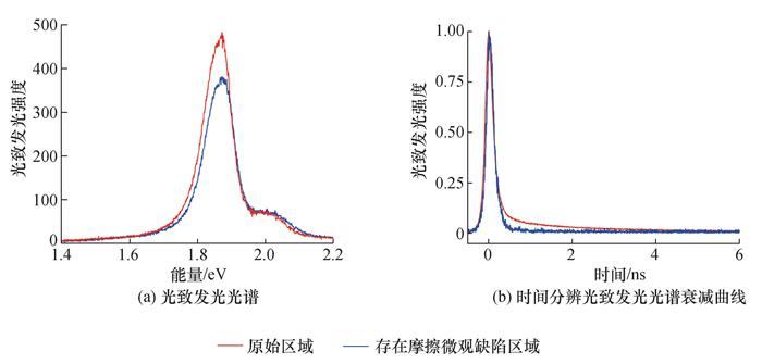
为了研究微观缺陷对单层MoS2发光特性的影响,首先进行了稳态光致发光光谱(Steady-State Photoluminescence Spectrum, SSPL Spectrum)的测试。实验使用532 nm波长的激光进行激发,通过100倍物镜聚焦至样品微区,使用的激光功率是27 μW。
为了揭示摩擦微观缺陷对荧光寿命的影响,使用时间分辨光致发光光谱(time-resolved photoluminescence, TRPL)技术来对样品的荧光寿命进行表征。借助脉冲激光进行激发,激光波长405 nm,重复频率40 MHz,通过100倍物镜(数值孔径0.8 NA, 厂家Olympus)聚焦激光和收集信号,经过长通滤波片(型号ET575LP, 厂家Chroma)滤除激光从而仅收集荧光信号。
为了研究摩擦微观缺陷在低温下对单层MoS2荧光特性的影响,进行变温光致发光光谱的测试。样品被放置在封闭循环低温系统中(型号CA50, 厂家Montana),波长为473 nm的激光通过自建的光路,经过100倍物镜(型号0.9 NA, 厂家Zeiss)聚焦至样品并收集荧光信号,激发功率是1 μW。

2 实验结果

2.1 摩擦微观缺陷的引入与验证

图 1c中,原始的MoS2有384 cm-1和402 cm-1 2个主要的峰,分别为MoS2的剪切模态E2g1和伸缩模态A1g,这与文[8-9]一致。而在进行过原子力探针摩擦产生缺陷的区域,观察到E2g1峰发生了红移,A1g峰发生了蓝移,这种变化表明,摩擦微观缺陷引入了额外的应力场和缺陷态。这与文[10-11]通过等离子轰击等手段产生微观缺陷后的Raman结果一致。这说明,通过探针的往复摩擦,已经产生微观的摩擦缺陷。

2.2 摩擦微观缺陷对光致发光特性的影响

图 2a展示了原始区域和存在摩擦微观缺陷区域的光致发光光谱结果。在1.85 eV处,可以观察到单层MoS2的荧光发射峰,这与文[12]一致。这是由于激光激发MoS2单层,材料中的电子吸收光子的能量,从基态跃迁到激发态,从而在导带中产生自由电子,同时在价带中留下一个空穴。在激发态下,位于激发态的电子在一段时间后会和空穴发生复合,释放特定波长的光子,产生荧光峰。存在摩擦微观缺陷区域的光致发光强度比原始区域显著降低。这是由于缺陷能级的引入形成了额外的非辐射复合路径,电子被缺陷态捕获后通过热耗散方式释放能量,从而降低了荧光效率,导致发光强度的变化或信号峰位的移动[13-14]
图 2 原始区域与摩擦微观缺陷区域的光致发光特性比较
不同扫描区域的TRPL衰减曲线及其对应的拟合曲线如图 2b所示。可以看到,存在摩擦微观缺陷区域的TRPL曲线衰减速度比原始区域的更快。2条TRPL曲线的前半段可以很好地进行单指数拟合[15-16]
$I_{(t)}=A_i \mathrm{e}^{-t / \tau_i} .$
其中Aiτi分别为第i个分量的振幅和衰减时间。通过拟合,发现室温下原始区域A激子寿命为0.198 ns,而存在摩擦微观缺陷区域的寿命降低为0.128 ns。这是由于在样品表面用原子力探针进行摩擦时,会导致样品损伤并在MoS2层中产生摩擦微观缺陷。这些摩擦微观缺陷形成缺陷能级,并能够捕获A激子中的电子,形成额外的能量耗散通道,这会显著减少A激子的布居数,从而降低其寿命[17-18]

2.3 温度和激发功率的影响

随着激发功率的增加,激光可以激发更多的载流子,促进了激子的生成和复合过程。由图 3可以看出,原始区域的A激子随着激光功率提高,其光致发光强度快速增加,且峰位出现部分蓝移。而在存在摩擦微观缺陷的区域,光致发光强度的增加会受到缺陷能级的限制,表现为其光致发光光谱(Photoluminescence, PL)中光致发光强度在相同功率下始终比原始区域更低。这是因为缺陷能级引入的非辐射复合通道会导致部分激子复合转化为热能释放,降低了激子的量子产率,因此在高功率下,光致发光强度的提升比原始区域更低。
图 3 不同功率下原始区域和存在摩擦微观缺陷区域的光致发光光谱
当激发功率增加时,激发的电子和空穴对的浓度会显著增加。这会导致材料局部的温度升高。高温可能会引起材料中晶格的热膨胀,进而影响电子的能量状态。这种热效应通常会导致能带间隔的变化,从而使得光致发光峰的能量发生红移[19]。当摩擦微观缺陷存在时,将会引入新的能态,缺陷能级位于导带和价带之间并且这些缺陷态可以捕获电子,从而影响载流子的动力学,进而影响样品的发光特性。图 4中,在高载流子密度下,缺陷能级可能成为非辐射复合的主要途径,导致激子或载流子的复合效率下降,非辐射损失增大。这会抑制激子浓度的增加,从而减小原本应该伴随载流子浓度增加而导致的红移程度,这与观察到的现象相符。
图 4 荧光特性随功率变化的分析
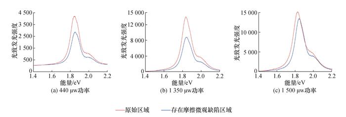
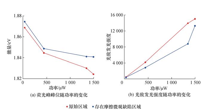
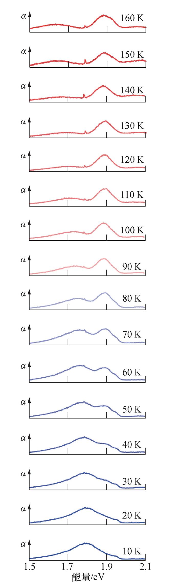
图 5中,以α表示归一化光致发光强度,在10~160 K温度范围,以10 K为步长测试了存在摩擦微观缺陷区域的MoS2单层的光致发光峰。可以看到,随着温度的下降,在1.65~1.8 eV逐渐出现半高宽更宽的荧光峰,这与文[20]相符,并将其标记为缺陷峰。随着温度降低至60 K,缺陷峰逐渐占据主导,且强度超过MoS2的A激子。这是因为摩擦微观缺陷会在带隙中引入额外的缺陷能级,形成额外的能量态,影响光致发光光谱的特征。这些缺陷态通常作为非辐射复合中心,降低了光致发光的量子效率。同时,低温下热激发效应减弱,激子更容易被缺陷态捕获,形成缺陷复合中心。由于非辐射复合路径的增多,导致A激子信号强度减弱而缺陷峰强度显著增强。这种现象说明,摩擦微观缺陷在低温下对载流子动力学和激子布居数的影响更加显著。这一结果为理解摩擦微观缺陷如何影响光电器件在低温条件下的工作性能提供了理论依据。
图 5 不同温度下存在缺陷区域的MoS2单层光致发光光谱

3 分析与讨论

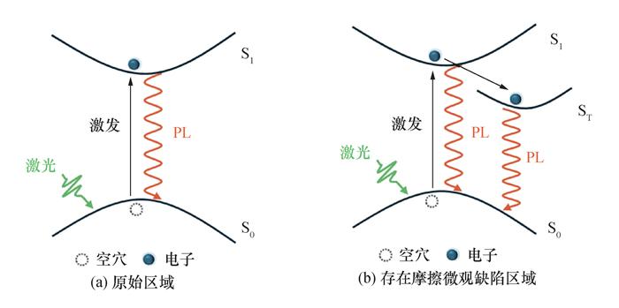
实验结果表明摩擦微观缺陷是引起MoS2单层中的荧光特性变化的重要原因,图 6总结了原始和存在摩擦微观缺陷的MoS2区域中可能出现的激子动力学过程。在原始区域,微观缺陷密度较小,激光激发样品价带S0中的电子后跃迁至导带S1,并在价带留下一个空穴;通过辐射复合电子和空穴释放光子,因此光致发光强度较高(见图 6a)。引入摩擦微观缺陷后,缺陷会捕获电子,形成缺陷能级ST,一些被激光激发的电子被缺陷所束缚(见图 6b)。此时缺陷能级的存在提供了非辐射复合通道,形成了额外的能量耗散通道,进而降低了样品的量子产率和寿命。在低温下时,由于热涨落影响降低,激子更容易被缺陷态捕获,导致缺陷峰可能主导光谱特征,低温下的光致发光光谱表现出明显的峰位移动。
图 6 原始区域和存在摩擦微观缺陷区域中可能出现的激子动力学过程
摩擦诱导的微观缺陷显著影响单层MoS2的激子动力学和发光特性。摩擦微观缺陷的存在引入了新的复合途径,缩短了激子的寿命,并且降低了光致发光强度。这样的变化意味着材料在应用于光电器件时,其发光效率和性能可能会降低,因此需要在实际应用中考虑摩擦微观缺陷的控制与优化。
本文验证了摩擦微观缺陷显著影响MoS2的光致发光特性,但这些结果是否适用于其他二维材料(如WS2、BN)仍需进一步研究。此外,实验条件(如探针类型、载荷大小)对缺陷生成的敏感性可能导致结果的局限性。未来可通过第一性原理计算和其他实验手段(如电子显微镜)对缺陷能级形成的具体机制进行深入研究。

4 结论

本文通过摩擦诱导微观缺陷的手段,系统揭示了摩擦微观缺陷对单层MoS2光致发光特性的影响。摩擦微观缺陷引入了新的缺陷能级,导致光致发光强度下降和激子寿命缩短。低温实验表明,缺陷峰在低温下主导光谱特征。研究结果阐明了微观缺陷对激子动力学和光学性能的关键影响,为优化光电器件的设计与性能提供了重要理论依据,同时强调了缺陷控制在高端材料应用中的重要性。
1
路新春, 温诗铸, 雒建斌. 微观摩擦磨损研究的新进展[J]. 摩擦学学报, 1995, 15 (2): 177- 183.

LU X C , WEN S Z , LUO J B . The new advance of micro friction and wear[J]. Tribology, 1995, 15 (2): 177- 183.

2
雒建斌, 郭东明, 杨华勇, 等. 原子级制造的关键基础科学问题[J]. 中国科学基金, 2024, 38 (1): 86- 98.

LUO J B , GUO D M , YANG H Y , et al. Key basic scientific issues in atomic level manufacturing[J]. Bulletin of National Natural Science Foundation of China, 2024, 38 (1): 86- 98.

3
FUJISAWA S , SUGAWARA Y , ITO S , et al. The two-dimensional stick-slip phenomenon with atomic resolution[J]. Nanotechnology, 1993, 4 (3): 138- 142.

DOI

4
YAMAMOTO T . Structure and friction of amorphous carbon films of nanometer thickness[J]. Wear, 1993, 168 (1-2): 27- 30.

DOI

5
GRILL A . Review of the tribology of diamond-like carbon[J]. Wear, 1993, 168 (1-2): 143- 153.

DOI

6
张军, 薛群基. LANGMUIR-BLODGETT膜及其摩擦行为[J]. 摩擦学学报, 1992, 12 (2): 97- 104.

ZHANG J , XUE Q J . LANGMUIR-BLODGETT film and its tribological behavior[J]. Tribology, 1992, 12 (2): 97- 104.

7
谭久彬, 蒋庄德, 雒建斌, 等. 高端精密装备精度测量基础理论与方法[J]. 中国科学基金, 2022, 36 (6): 955- 962.

TAN J B , JIANG Z D , LUO J B , et al. Accuracy measurement theory and method for high-end precision equipment[J]. Bulletin of National Natural Science Foundation of China, 2022, 36 (6): 955- 962.

8
FENG J J , FAN Y W , ZHAO H , et al. The first principles calculation on the Raman spectrum and optical properties of the defect monolayer MoS2[J]. Brazilian Journal of Physics, 2021, 51 (3): 493- 498.

DOI

9
LI H , ZHANG Q , YAP C C R , et al. From bulk to monolayer MoS2: Evolution of Raman scattering[J]. Advanced Functional Materials, 2012, 22 (7): 1385- 1390.

DOI

10
MIGNUZZI S , POLLARD A J , BONINI N , et al. Effect of disorder on Raman scattering of single-layer MoS2[J]. Physical Review B, 2015, 91 (19): 195411.

DOI

11
MAGUIRE P , FOX D S , ZHOU Y B , et al. Defect sizing, separation, and substrate effects in ion-irradiated monolayer two-dimensional materials[J]. Physical Review B, 2018, 98 (13): 134109.

DOI

12
RODRIGUEZ A , KALBÁAČ G M , FRANK O . Strong localization effects in the photoluminescence of transition metal dichalcogenide heterobilayers[J]. 2D Materials, 2021, 8 (2): 025028.

DOI

13
OH H M , HAN G H , KIM H , et al. Photochemical reaction in monolayer MoS2 via correlated photoluminescence, Raman spectroscopy, and atomic force microscopy[J]. ACS Nano, 2016, 10 (5): 5230- 5236.

14
LIU H , WANG C , LIU D M , et al. Neutral and defect-induced exciton annihilation in defective monolayer WS2[J]. Nanoscale, 2019, 11 (16): 7913- 7920.

15
XU L J , DUAN W R , LIU Y S , et al. Twist-angle- controlled neutral exciton annihilation in WS2 homostructures[J]. Nanoscale, 2022, 14 (14): 5537- 5544.

16
XU H W , WANG J C , LIU H , et al. Control of hybrid exciton lifetime in MoSe2/WS2 Moiré heterostructures[J]. Advanced Science, 2024, 11 (34): 2403127.

17
LIU H , WANG J C , LIU Y S , et al. Visualizing ultrafast defect-controlled interlayer electron-phonon coupling in van der waals heterostructures[J]. Advanced Materials, 2022, 34 (33): 2106955.

18
LIU H , WANG C , ZUO Z G , et al. Direct visualization of exciton transport in defective few-layer WS2 by ultrafast microscopy[J]. Advanced Materials, 2020, 32 (2): 1906540.

19
KO P J , ABDERRAHMANE A , THU T V , et al. Laser power dependent optical properties of mono-and few-layer MoS2[J]. Journal of Nanoscience and Nanotechnology, 2015, 15 (9): 6843- 6846.

20
ZHANG X M , XU J H , ZHI A M , et al. Low-defect-density monolayer MoS2 wafer by oxygen-assisted growth-repair strategy[J]. Advanced Science, 2024, 11 (42): 2408640.

Outlines

/